User:Monak
From 2006.igem.org
(→<font color='blue'>Smart materials from DNA</font color>) |
(→<font color='blue'>Smart materials from DNA</font color>) |
||
| (2 intermediate revisions not shown) | |||
| Line 30: | Line 30: | ||
==== <font color='blue'>Smart materials from DNA</font color> ==== | ==== <font color='blue'>Smart materials from DNA</font color> ==== | ||
| - | DNA-origami-sensor [[image:3fold_small.jpg|left|thumb|200px| | + | DNA-origami-sensor [[image:3fold_small.jpg|left|thumb|200px| DNA-origami-sensor]] |
For example by self-assembly of folded and connected DNA sheets, which will change their physical properties with environmental changes, e.g. ion-concentration or pH. | For example by self-assembly of folded and connected DNA sheets, which will change their physical properties with environmental changes, e.g. ion-concentration or pH. | ||
Sensing by means of conformational changes induced by changes in the DNA-orgigami-sensor environment can be based on the following two principles: | Sensing by means of conformational changes induced by changes in the DNA-orgigami-sensor environment can be based on the following two principles: | ||
| + | |||
1. Change in spacing between sheets of DNA as a reaction to stronger or weaker inter-sheet repulsion/attraction | 1. Change in spacing between sheets of DNA as a reaction to stronger or weaker inter-sheet repulsion/attraction | ||
| - | 2. Change in length of the connecting staples, e.g. by integration of parts like Part:BBa_J35120 that are capable of undergoing a BZ-Transformation => Co-sensor! [http://partsregistry.org/Part:BBa_J35120 Click here to have a look at Part:BBa_J35120] | + | |
| + | 2. Change in length of the connecting staples, e.g. by integration of parts like Part:BBa_J35120 that are capable of undergoing a BZ-Transformation => Co-sensor! (many thanks to our mutant-leader ak) | ||
| + | |||
| + | [http://partsregistry.org/Part:BBa_J35120 Click here to have a look at Part:BBa_J35120] | ||
<br style="clear:both;"/> | <br style="clear:both;"/> | ||
Latest revision as of 11:13, 28 October 2006
- Design Rules -
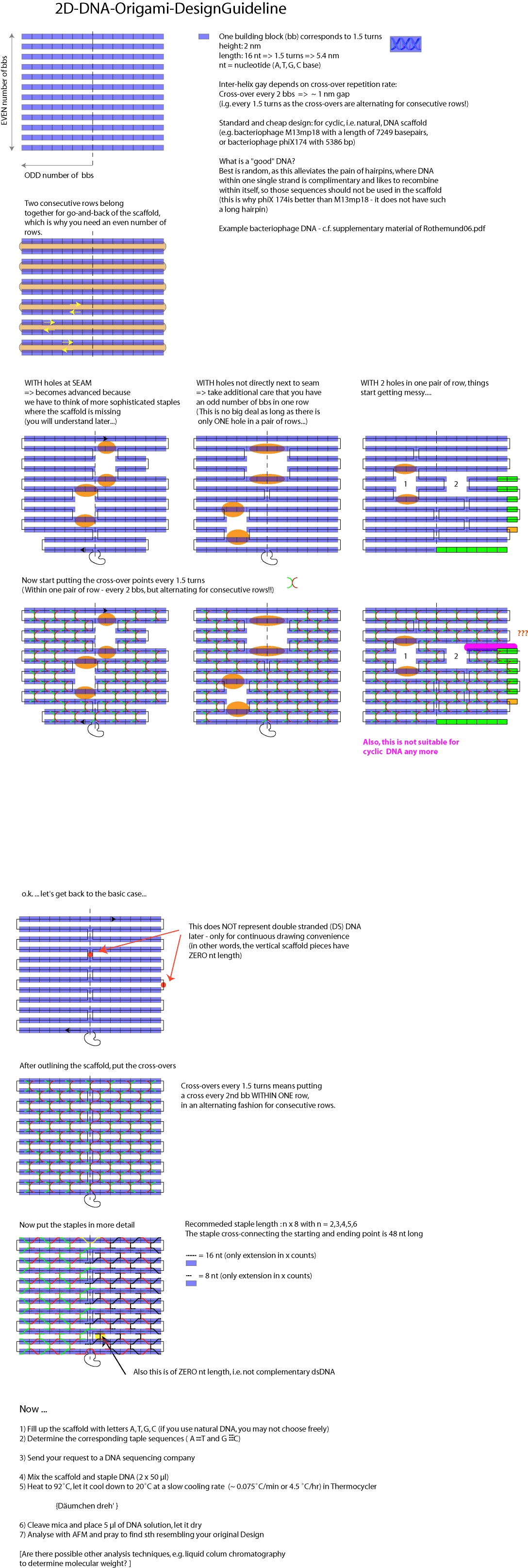
To get it clear for myself (as a person without any prior knowledge about the steric hybridization properties of DNA), I tried to set up some simple, engineering point-of-view rules for designing a plain sheet of DNA.
- 2D DNA sheet of more or less arbitrary shape (click here for high-resolution image)
- Individual project -
Wafer level nano-resolution pattern transfer
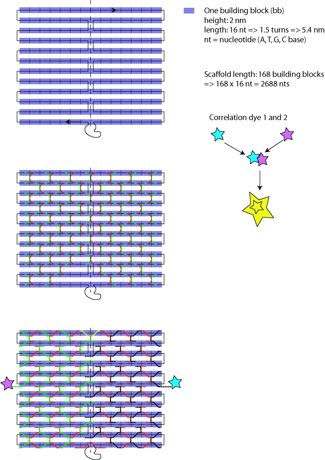
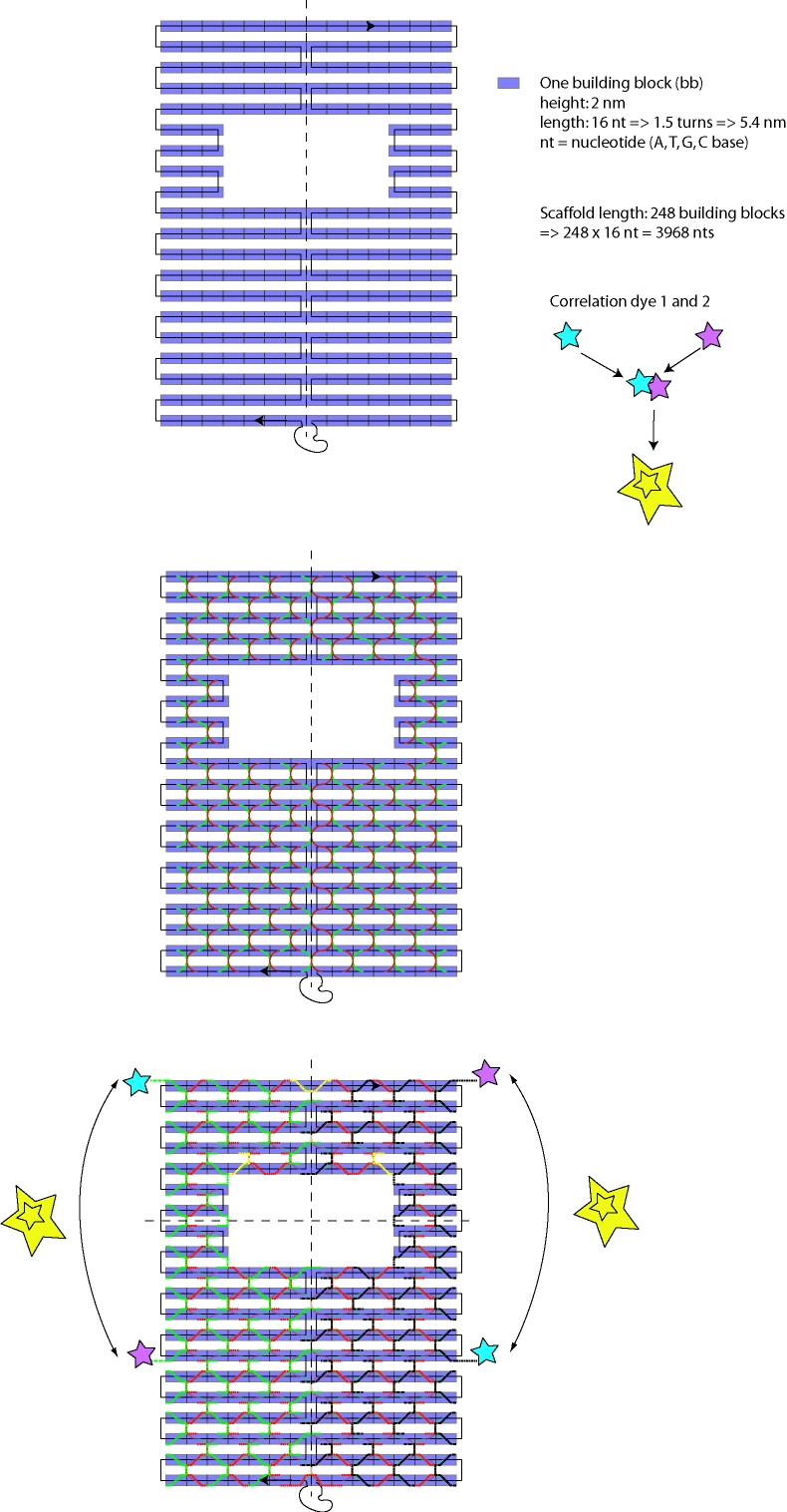
To start from the very basics, produce a plane sheet, and a sheet that folds once. For double-checking possibilitiy, we included a step-height variation that should appear in the AFM image, and a correlation fluorescence dye.
The plain sheetThis shall be the kick-off starting point to get into the business of DNA origami and employing it for nm-scale pattern transfer.
The upper part is not as long as the lower part so as to have two ways for checking if the DNA has folded correctly or not.
1. The step should be visible in the AFM image
2. We should be able to get a high signal for correlation fluorescence microscopy.
Pattern transfer
It's a hot business, and we have to admit that we have no profound basis WHAT technique might work, but a lot of ideas & the corresponding equipment to try out many different ways.
Smart materials from DNA
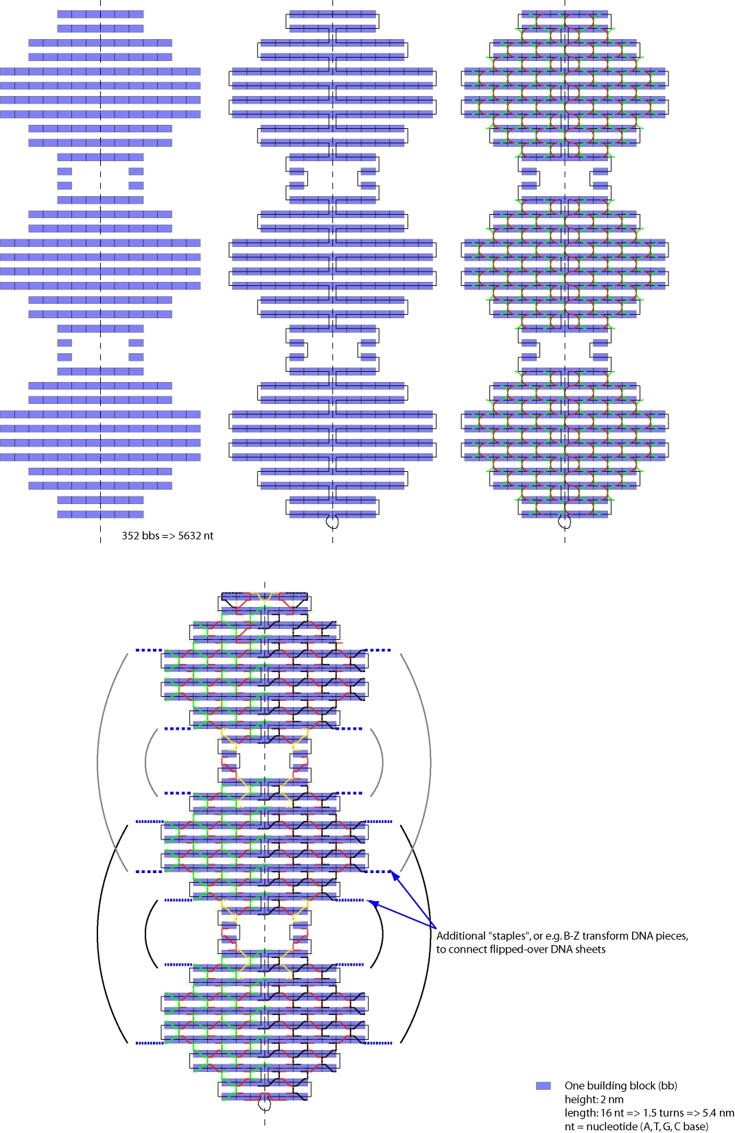
DNA-origami-sensorFor example by self-assembly of folded and connected DNA sheets, which will change their physical properties with environmental changes, e.g. ion-concentration or pH.
Sensing by means of conformational changes induced by changes in the DNA-orgigami-sensor environment can be based on the following two principles:
1. Change in spacing between sheets of DNA as a reaction to stronger or weaker inter-sheet repulsion/attraction
2. Change in length of the connecting staples, e.g. by integration of parts like Part:BBa_J35120 that are capable of undergoing a BZ-Transformation => Co-sensor! (many thanks to our mutant-leader ak)
[http://partsregistry.org/Part:BBa_J35120 Click here to have a look at Part:BBa_J35120]
- Personal information -
e-mail: mona.klein@imtek.uni-freiburg.de
Education
Just graduated from the department of Microsystems Engineering.
Diploma-thesis (corresponds to a 6-month compressed master's thesis) dealt with the fabrication of a solenoidal coil for MRI of cells.
Title: Fabrication of a Solenoidal Coil with Integrated Sample Container for Micro-MRI
[http://2006.igem.org/wiki/index.php/Freiburg_University_2006 Home]


